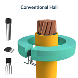
IMC-Hall® current sensing
We explain here the basis of the IMC-Hall technology and the benefits it brings to current sensing. Since it is based on the Hall-effect principle, you might be interested in starting your journey here.
IMC-Hall sensing technology
IMC-Hall concept
Hall effect technology is deployed in the field of current sensing, magnetic position sensing and earth magnetic field sensors (also known as electronic compasses). The strength of the Hall effect technology is that it can be integrated into standard CMOS processes, making it a very cost effective sensing technology.
Melexis also has a proprietary Integrated Magnetic Concentrator (IMC) technology which locally converts the horizontal magnetic field (Bx) into a vertical component (Bz) that can be measured with those high performing silicon Hall plates.

This small animation illustrates the magnetic field lines generated by the current flowing through the bus bar.
It shows how the lines are impacted by the elements:
-
The shield concentrates the field within an area.
-
The IMC (from the IC) “bend ” and concentrates the field lines so it can be perceived by the horizontal Hall plates (from the IC)

Focusing on the IMC itself, here is an example of its influence (yellow disk is the IMC)
An immediate advantage of the IMC, on top of the flexibility it brings, is a magnetic gain which is proportional to its size.
IMC-Hall versus mechanical tolerances

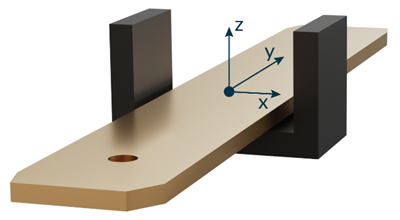
When it comes to current sensing, mechanical design considerations play an important role in the choice of technology. The position of the current conductor versus the sensor results in a multitude of possibilities, and it is exactly where the IMC-Hall® technology brings several advantages over classic core-based solutions.
First, it allows an elegant vertical stacking of the current conductor (that can also be embedded in the PCB), the PCB and the sensing IC. This is particularly interesting for embedded applications where the current sensor IC is part of a bigger PCB with other components. It facilitates the assembly process, especially when intermediate assembly is performed by a TIER.
Secondly, surface mount packages can be employed since the sensing direction is parallel to the IC. It enables simpler PCB assembly process which saves cost.
For comparison, core-based technologies require the use of through-hole packages which make them not suited for vertical stacking. They attempt to achieve surface mounting capabilities of the IC using more expensive lead bending techniques. Sometimes plastic holders are even required to pass vibration tests (mechanical robustness specifications). Vibrations can be seen as a form of mechanical play, which in turn also influences the magnetic signal obtained from the current measurement. IMC-Hall technology is a more robust solution in terms of mechanical play.
Discover more in the Melexis reference design guide.
IMC size
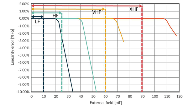
IMC-Hall® sensors are available in 4 different versions/sizes covering a broad range of sensitivities and magnetic field ranges: Low Field (LF), High Field (HF), Very High Field (VHF), Extra High Field (XHF).
With its strong magnetic gain, the biggest IMC (LF) is ideally suited for applications with low currents, requiring high magnetic sensitivities (up to 700mV/mT). At the other end of the spectrum, the smallest IMC (XHF) can linearly sense strong magnetic fields up to ±90mT, for current sensing applications with very high-power densities.
| IMC type | Current range |
| LF (low field) | [0A – 200A] |
| HF (high field) | [100A – 700A] |
| VHF (very high field) | [200A – 1400A] |
| XHF (extra high field) | [500A – 2000A] |
The conversion of the magnetic field domain of each IMC size into a current range highly depends on the shield dimensions. By combining the data of shields with a width up to 30mm, we can define a current range for each IMC.
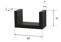
Terminology for the shield geometry:
L = length
W = width
T = thickness
H = height
Stray fields immunity
Stray fields
One of the challenges in designing magnetic sensors, is that they should provide an output proportional to the magnetic flux density generated by the current to be measured, while at the same time be as insensitive as possible to other sources of magnetic fields surrounding the sensor, the so-called “stray fields”. This is because a sensor measuring the magnetic field along a single axis, is not able to discriminate between the contributing sources of the measured aggregate magnetic field. These stray fields find their origin in other nearby currents flowing (so-called crosstalk), nearby permanent magnets and finally - to a much lesser extent - the earth magnetic field. Since there is no means of curing the presence of stray fields, one can only prevent them from reaching the sensor. The influencing design variables are the following:
1) Stray field avoidance
Keep stray field sources as far as possible of the sensor. Remember that magnetic field decay is inversely proportional with the distance (as per Biot-Savart's law). This is a very powerful option and unfortunately often overlooked despite its obviousness. It is also often seen as in contradiction with the request to downsize the module for miniaturization and cost reasons. Those requirements are actually not necessarily incompatible, especially when decisions in the mechanical design process are taken with the consideration of the sensor designer’s challenges in view of stray field immunity.
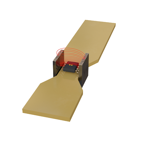
One source of stray field among others might be an adjacent busbar. The picture below shows the magnetic field measured at the sensor generated by an adjacent conductor. This adjacent conductor is placed at a distance between 20 mm and 170 mm. Two simulations have been done: with the optimal position and with the sensor placed 1 mm above its optimal position.
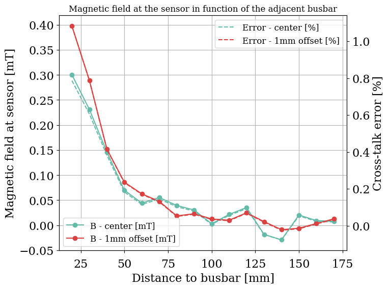
Simulations have been done with a LU15-13-15-3 shield from Maglab.
Other shield dimensions will have similar results.
One can clearly see an exponential decrease. The higher the sensor in the shield, the higher its sensitivity to external field (red line starts above green line). It is therefore recommended to keep the sensor as much as possible inside the shield and to keep adjacent busbars or any other stray field source as far as possible.
It is also important to understand what kind of error the stray field is causing.
- A random stray field is contributing to the offset error - if you measure 0A or 1000A the stray field error will remain the same.
- However, if the stray field is generated by an adjacent bus bar, it might not be an offset error. If the current of the adjacent bus bar is linked to the current to be measured, as for example in the case of a bus bar that does a U-turn, the stray field error will be proportional to the current. In this case it contributes to the sensitivity error (i.e. at 0A there is 0mT stray field).
2) Stray field rejection
Use a ferromagnetic shield and make it as narrow as possible, which has a double effect:
- First, it will provide more signal, which in turn will also increase the signal to external stray field ratio.
- Second, the more narrow the so-called airgap, the higher the stray field immunity. The detour of the magnetic stray field through the permeability shield becomes more attractive than going through the sensor itself using a path of low permeability (or high magnetic resistance aka reluctance) through air instead.
The parameter that quantifies this immunity to external stray fields is the Shielding Factor (SF). The higher factor, the higher stray field immunity. It is defined as the ratio between a homogenous magnetic field applied externally (Bext) and the attenuated magnetic field measured at the sensor position (Bint). A typical (representative) stray field used in the industry is 1.25mT, finding its origin in 1000A/m (ISO 11452-8). Essentially it depends from the system and the choices made according to the first paragraph describing the stray field sources.
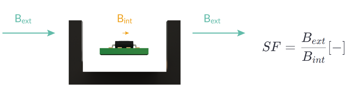
Note that no current is involved here since we only look at the stray field and its impact. A SF of 10 means that the sensor measures 10 times less field than in the environment.
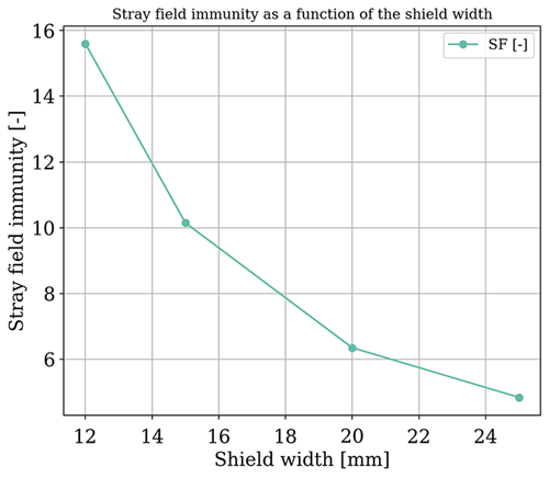
This picture shows the importance of keeping the shield width as small as possible, forcing sometimes to reduce the busbar width locally. This geometry, also shown on the right picture, is called a neckdown and improves the sensor performance in two ways:
- the IC sense more magnetic field which increases the SNR
- better shielded against stray fields
This is why Melexis recommends using shields with a width of 12mm or 15mm.
Mechanical tolerances and assembly
Mechanical tolerances
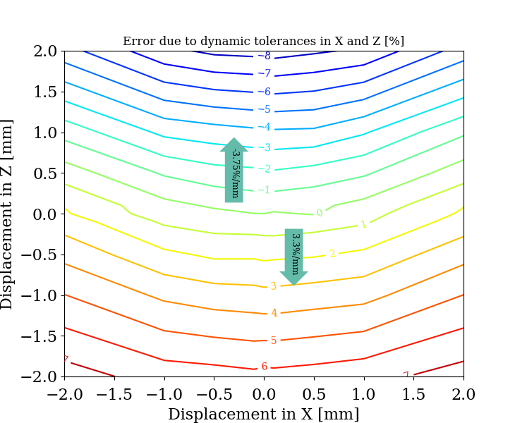
While any error due to displacement during the assembly (also called static tolerances) can be compensated, the dynamic tolerances can't be. The IMC-Hall technology is the most robust open loop Hall solution against mechanical tolerances.
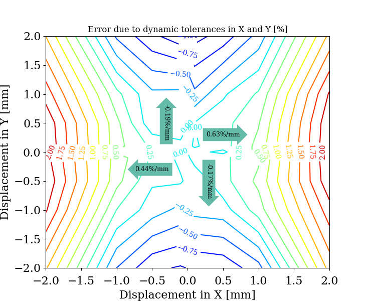
Simulations have been done with a LU15-13-15-3 shield from Maglab.
Other shield dimensions will have similar orders of magnitude between X, Y and Z displacement
In the table below, one can see an approximation of the error for the three directions, X, Y and Z. One can clearly see that the less sensitive direction is along the shield length (Y) and the most sensitive one is along the shield height (Z). It is fair to assume a factor 3 between the error along the Y and the X axis and a factor of 15 between the error along the Y and Z axis.
| Direction | Value |
| X | ~0.6 %/mm |
| Y | ~0.2 %/mm |
| Z | ~3.5 %/mm |
In other words, a displacement of 0.1mm along the z-axis induces a similar error as a displacement of 1.5mm along the y-axis.
The conclusion is that the IMC-Hall technology is very robust against mechanical tolerances in X and Y. For an optimal design it is recommended to strengthen the fixation along the z-axis by placing the fixation screws close to the sensor and shield assembly.
Mechanical assembly
For the best practices, discover our guidelines on how to assemble the IC on a PCB at PCB assembly.
Module calibration
Melexis proposes magnetically calibrated ICs with a few different standard sensitivities, expressed in mV/mT. Most of the time these standard variants can be used as is and does not require any EOL (end of line) calibration.
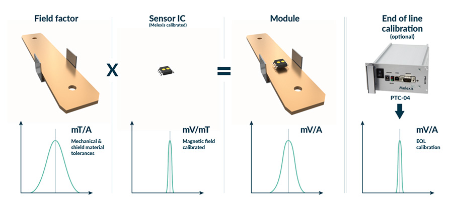
Further compensations are possible for better end-accuracy:
- via PTC-04 EOL calibration
By applying two currents (0 A and a positive current for instance), the PTC-04 programmer recalibrates the IC by updating its EEPROM. - via a microcontroller
By applying two currents (0 A and a positive current for instance) the microcontroller can correct the offset and the slope of the sensor measurement. This is a common approach to reject module tolerances (assembly, shield material tolerances…). It also allows you to calculate the measured current based on the IC output voltage, without doing an EOL calibration.
Discover more: Calibration and Programming documentation
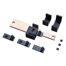
Evaluation kits
Melexis offers a dedicated development kit (DVK): the DVK-IMC-Hall-Shield. This kit provides all you need to evaluate the IMC-Hall current sensor ICs.
Discover more with the Evaluation kits documentation


